Scanning Tunneling and Atomic Force Microscopes
Scanning Tunneling and Atomic Force Microscopes
An ordinary microscope, which employs optical lenses, cannot be used to view objects smaller than the wavelength of light. An electron microscope can view smaller things with greater clarity than an optical microscope, but still cannot clearly view individual atoms. Today, scientists and engineers can visualize things even smaller than individual atoms by using an instrument called the scanning tunneling microscope or STM.
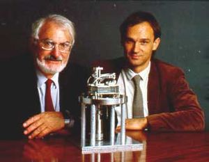
Gerd Binnig and Heinrich Rohrer, two researchers working for the IBM Corporation, designed the first STM in 1981. The original STM microscope examined small samples of matter held in a refrigerated chamber. At –455 °F (–271 °C) in the chamber, the natural tendency of atoms to move around slows almost to a halt. To keep gasses in the air from knocking against the atoms in the sample, all the air in the chamber is pumped out. In addition, stray magnetic fields that might push and pull on the sample’s atoms are blocked out by the chamber’s metal housing.
Inside the chamber, a tiny stylus with a tip just one atom wide (made by new micromachining techniques) is slowly moved over the surface of the object to be scanned by a special robotic arm. A small electric current carried to the tip begins to flow between the tip and the sample. This current increases as the tip gets closer to the surface of the object. Measuring the flow of current provides a precise indication of the distance from the tip to the individual atoms on the surface of the sample. Computers are then used to translate this data into an image that can be displayed on a monitor. Other researchers later discovered that the STM could also be used to push and pull individual atoms around, marking the first time that humans could manipulate objects that small.
A shortcoming of the original STM was the fact that only conductive surfaces like metals could be used with it. In 1986, five years after the STM’s invention, Binnig, Christoph Gerber, and Calvin Quate invented the atomic force microscope (AFM). This device also uses a tiny stylus that is slowly moved over the surface of a sample object or material. The stylus is attached to a flexible arm called a cantilever, and as minute atomic forces attract or repel the stylus, the stylus is pushed toward or pulled away from the sample. This also moves the cantilever. A special laser aimed at the cantilever is reflected, and the angle of reflection changes as the cantilever moves. Then an electronic detector senses the movement of the beam and a computer imaging system creates an image of the surface of the sample on a monitor. Because the AFM stylus touches the sample, it can be used with nonconductive surfaces and can also be used like the STM to position objects as small as an atom. This fact has led experimenters to begin working on the use of the AFM or a similar system to construct miniscule machines and electronic devices, such as transistors.
About a dozen similar types of instruments have joined the STM and AFM in the past ten years. Taken together, these devices have revolutionized the study of materials and have confirmed many theories about atoms that were not previously observable.
