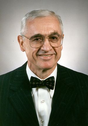
Nick Holonyak, Jr.
Biography
Nick Holonyak, Jr. was born in Zeigler, Illinois on 3 November 1928. He received the B.S., M.S., and Ph.D. in Electrical Engineering from the University of Illinois in 1950, 1951, and 1954, respectively. As a Texas Instruments Fellow in Semiconductor Physics at the University of Illinois (1953-54), he did graduate work under the direction of John Bardeen.
Dr. Holonyak joined the Technical Staff at Bell Telephone Laboratories, Murray Hill, NJ in 1954. His work there included demonstration of the feasibility of the first diffused-impurity silicon devices. From 1955-57 he served with the U.S. Army Signal Corps and in 1957 joined the Advanced Semiconductor Laboratory of the General Electric Company in Syracuse, NY where he made important inventions and key contributions in the area of advanced semiconductor devices, including the invention of the first visible semiconductor laser.
In 1963, Dr. Holonyak moved to the University of Illinois where he is currently Professor in the Department of Electrical and Computer Engineering and Materials Research Laboratory, and a member of the Center for Advanced Study. Dr. Holonyak has been responsible for several important breakthroughs, particularly in the area of crystal preparation of compounds and ternary alloys, light-emitting diodes, and semiconductor lasers. Since 1976, he has conducted extensive research on quantum-well and other novel light-emitting structures.
Dr. Holonyak has been granted sixteen patents in the field, is the author/co-author of over 380 technical articles and two books. He is the editor of the Prentice-Hall series "Solid State Physical Electronics," has served on the editorial boards of the PROCEEDINGS of the IEEE, SOLID-STATE ELECTRONICS, and the JOURNAL OF APPLIED PHYSICS AND APPLIED PHYSICS LETTERS, and is a member of the Board of Editorial Associates of SEMICONDUCTORS AND INSULATORS.
Dr. Holonyak's contributions have been recognized by receipt of the following awards: the General Electric Company Cordiner Award (1962); the IEEE Morris N. Liebmann Award (1973); the John Scott Medal of the City of Philadelphia (1975); the GaAs Symposium Award with Welker Medal (1976); the IEEE Jack A. Morton Award (1981); the Solid State Science and Technology Award of the Electrochemical Society (1983); Sigma Xi Monie A. Ferst Award (1988). He is a member of the National Academy of Engineering, the National Academy of Sciences, a Fellow of the IEEE, the American Academy of Arts and Sciences, and the American Physical Society. He has served on various IEEE, AIP, APS and NAS committees. At the invitation of the U.S.S.R. Academy of Sciences, he has visited laboratories in the Soviet Union (1967, 1974), and in 1956-57 was a regular seminar speaker at the laboratory of Makoto Kikuchi of the Electrotechnical Laboratory (Tokyo). He was awarded the 1989 IEEE Edison Medal 'For an outstanding career in the field of electrical engineering with contributions to major advances in the field of semiconductor materials and devices.'
Apart from his work and interests in semiconductor materials and devices, and research with his graduate students, Nick Holonyak enjoys reading, and some running and weightlifting. He is fluent in a second language, the Carpatho-Russian of his immigrant parents. His wife Katherine is a member of the nursing profession.
