NanoInk: Difference between revisions
No edit summary |
No edit summary |
||
| Line 1: | Line 1: | ||
== NanoInk == | == NanoInk == | ||
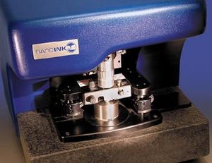
[[Image:Nanoink.jpg|thumb|left|NanoInk Corporation believes that its “Nscriptor” system for producing nanoscale structures will be a stepping stone to future nanomanufacutring. Source: NanoInk.]] | [[Image:Nanoink.jpg|thumb|left|NanoInk Corporation believes that its “Nscriptor” system for producing nanoscale structures will be a stepping stone to future nanomanufacutring. Source: NanoInk.]] | ||
Practical nanoink systems were introduced in 2002 by NanoInk Corporation, a company formed to take advantage of Mirkin’s inventions. The company’s nanolithography systems utilize multiple writing tips, made on flexible cantilevers using processes similar to the manufacture of MEMS and other semiconductors. One of the first commercial applications for the systems was in the repair of defective silicon wafers, onto which microchips are made. Defects in production normally can not be easily repaired, but nanoink lithography offers a way to do that. Future applications will, the company says, move toward true nanotechnological applications. | In the race toward nanotechnology, the NanoInk Corporation has put itself in the running. One of the main obstacles to designing more complex nanotechnologies is that building up machines, chemicals or other structures atom-by-atom has never been done before. While some are using the Atomic Force Microscope to move individual atoms around, or are designing self-assembling molecules through large-scale chemical reactions, NanoInk and others are taking another approach. NanoInk is both the name of the company and a new technology for building things at the atomic level. It is based on the work of a chemist named Chad Mirkin, who is a professor at Northwestern University. In the late 1990s, Mirkin discovered a way to use a device much like an Atomic Force Microscope to deposit tiny amounts of material on a surface in a very precise way. The tip of the microscope can be dipped into a solution containing one or more chemicals or compounds, picking up a droplet. Then, when the AFM tip is moved to the surface at the desired spot, the droplet forms a sort of bridge or link between tip and surface, greatly improving the accuracy with which materials in the solution can be deposited. The process is like a microscropic version of the ink and quill used for writing before the 20th century. By combining this with other techniques, Mirkin’s “dip pen lithography” could build up tiny nanostructures with relative ease. | ||
Practical nanoink systems were introduced in 2002 by NanoInk Corporation, a company formed to take advantage of Mirkin’s inventions. The company’s nanolithography systems utilize multiple writing tips, made on flexible cantilevers using processes similar to the manufacture of [[MEMS|MEMS]] and other semiconductors. One of the first commercial applications for the systems was in the repair of defective silicon wafers, onto which microchips are made. Defects in production normally can not be easily repaired, but nanoink lithography offers a way to do that. Future applications will, the company says, move toward true nanotechnological applications. | |||
[[Category:Engineered_materials_&_dielectrics|Category:Engineered_materials_&_dielectrics]] [[Category:Nanotechnology]] [[Category:Nanoscale_devices]] | [[Category:Engineered_materials_&_dielectrics|Category:Engineered_materials_&_dielectrics]] [[Category:Nanotechnology]] [[Category:Nanoscale_devices]] | ||
Revision as of 21:45, 26 January 2009
NanoInk
In the race toward nanotechnology, the NanoInk Corporation has put itself in the running. One of the main obstacles to designing more complex nanotechnologies is that building up machines, chemicals or other structures atom-by-atom has never been done before. While some are using the Atomic Force Microscope to move individual atoms around, or are designing self-assembling molecules through large-scale chemical reactions, NanoInk and others are taking another approach. NanoInk is both the name of the company and a new technology for building things at the atomic level. It is based on the work of a chemist named Chad Mirkin, who is a professor at Northwestern University. In the late 1990s, Mirkin discovered a way to use a device much like an Atomic Force Microscope to deposit tiny amounts of material on a surface in a very precise way. The tip of the microscope can be dipped into a solution containing one or more chemicals or compounds, picking up a droplet. Then, when the AFM tip is moved to the surface at the desired spot, the droplet forms a sort of bridge or link between tip and surface, greatly improving the accuracy with which materials in the solution can be deposited. The process is like a microscropic version of the ink and quill used for writing before the 20th century. By combining this with other techniques, Mirkin’s “dip pen lithography” could build up tiny nanostructures with relative ease.
Practical nanoink systems were introduced in 2002 by NanoInk Corporation, a company formed to take advantage of Mirkin’s inventions. The company’s nanolithography systems utilize multiple writing tips, made on flexible cantilevers using processes similar to the manufacture of MEMS and other semiconductors. One of the first commercial applications for the systems was in the repair of defective silicon wafers, onto which microchips are made. Defects in production normally can not be easily repaired, but nanoink lithography offers a way to do that. Future applications will, the company says, move toward true nanotechnological applications.
