Milestones:Semiconductor Planar Process and Integrated Circuit, 1959: Difference between revisions
No edit summary |
No edit summary |
||
| Line 1: | Line 1: | ||
[[Image:Planar process IC dedication.JPG|thumb|left]] | [[Image:Planar process IC dedication.JPG|thumb|left]] | ||
== Semiconductor Planar Process and Integrated Circuit, 1959 == | |||
''The 1959 invention of the Planar Process by Jean A. Hoerni and the | ''The 1959 invention of the Planar Process by Jean A. Hoerni and the Integrated Circuit (IC) based on planar technology by [[Robert Noyce|Robert N. Noyce]] catapulted the semiconductor industry into the silicon IC era. This pair of pioneering inventions led to the present IC industry, which today supplies a wide and growing variety of advanced semiconductor products used throughout the world.'' | ||
By the early 1950s, scientists and engineers first conceived of entire electronic circuits formed within a single block of semiconductor material. In the spring of 1959, several individuals filed key patent applications in pursuit of this goal. In his miniaturized electronic circuits, [[Jack Kilby|Jack Kilby]] of Texas Instruments used only one kind of material to fabricate all circuit elements. Kurt Lehovec of Sprague Electronics claimed the use of P-N junctions for the electrical isolation of such elements. At Fairchild Semiconductor, Jean Hoerni’s revolutionary planar process inspired Robert Noyce’s vision of interconnecting multiple elements on a chip without manual wiring. And late in 1959, Jay Last assembled a team whose creative efforts led in 1960 to the development of Fairchild Micrologic, the first planar integrated circuits and the forerunners of the modern world of microelectronics. | |||
[[Media:3025589 Hoerni.pdf|US Patent 3025589 filed 1 May 1959 (Hoerni) ]] and [[Media:2981877 Noyce.pdf|US Patent 2981877 (Noyce)]] filed 30 July 1959 are attached. | |||
US Patent 3025589 filed 1 May 1959 (Hoerni) [[ | |||
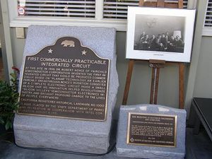
The IEEE Milestone plaque may be visited at the original Fairchild Semiconductor Offices, a marked historical site, at 844 East Charleston Rd., Palo Alto, California, U.S.A. | The IEEE Milestone plaque may be visited at the original Fairchild Semiconductor Offices, a marked historical site, at 844 East Charleston Rd., Palo Alto, California, U.S.A. | ||
[[Category:Components,_circuits,_devices_&_systems|Category:Components,_circuits,_devices_&_systems]] [[Category:Integrated_circuits|Milestones:Semiconductor Planar Process and Integrated Circuit, 1959]] | [[Category:Components,_circuits,_devices_&_systems|Category:Components,_circuits,_devices_&_systems]] [[Category:Integrated_circuits|Milestones:Semiconductor Planar Process and Integrated Circuit, 1959]] | ||
Revision as of 17:02, 16 September 2009
Semiconductor Planar Process and Integrated Circuit, 1959
The 1959 invention of the Planar Process by Jean A. Hoerni and the Integrated Circuit (IC) based on planar technology by Robert N. Noyce catapulted the semiconductor industry into the silicon IC era. This pair of pioneering inventions led to the present IC industry, which today supplies a wide and growing variety of advanced semiconductor products used throughout the world.
By the early 1950s, scientists and engineers first conceived of entire electronic circuits formed within a single block of semiconductor material. In the spring of 1959, several individuals filed key patent applications in pursuit of this goal. In his miniaturized electronic circuits, Jack Kilby of Texas Instruments used only one kind of material to fabricate all circuit elements. Kurt Lehovec of Sprague Electronics claimed the use of P-N junctions for the electrical isolation of such elements. At Fairchild Semiconductor, Jean Hoerni’s revolutionary planar process inspired Robert Noyce’s vision of interconnecting multiple elements on a chip without manual wiring. And late in 1959, Jay Last assembled a team whose creative efforts led in 1960 to the development of Fairchild Micrologic, the first planar integrated circuits and the forerunners of the modern world of microelectronics.
US Patent 3025589 filed 1 May 1959 (Hoerni) and US Patent 2981877 (Noyce) filed 30 July 1959 are attached.
The IEEE Milestone plaque may be visited at the original Fairchild Semiconductor Offices, a marked historical site, at 844 East Charleston Rd., Palo Alto, California, U.S.A.
