Milestones:First Practical Field Emission Electron Microscope, 1972: Difference between revisions
No edit summary |
|||
| (11 intermediate revisions by one other user not shown) | |||
| Line 1: | Line 1: | ||
== First Practical Field Emission Electron Microscope, 1972 == | == First Practical Field Emission Electron Microscope, 1972 == | ||
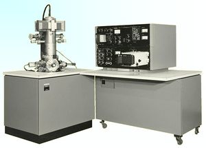
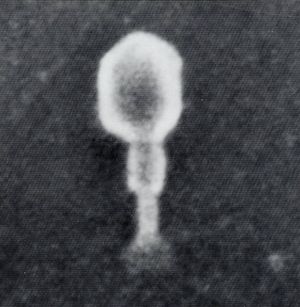
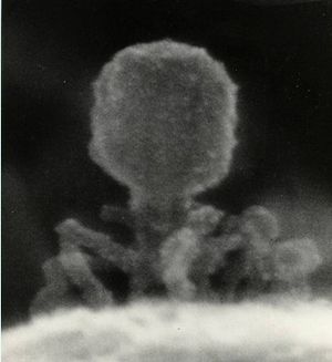
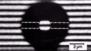
'' | ''Hitachi developed practical field emission electron source technology in collaboration with Albert Crewe of the University of Chicago, and commercialized the world’s first field emission scanning electron microscope in 1972. This technology enabled stable and reliable ultrahigh resolution imaging with easy operation. Field emission electron microscopes have made invaluable contributions to the progress of science, technology and industry in physics, biology, materials, and semiconductor devices.'' [[Image:Hitachi 1972 FE-SEM HFS-2.jpg|thumb|right|Photo 1: Hitachi's Wolrd First Commercial FE-SEM (model HFS-2), 1972]][[Image:Crewe 1972 T2-bacteriophages.jpg|thumb|right|Photo 2a: Observation of T2-bacteriophages, Prof. A. V. Crewe, 1972, Equipment: HFS-2 FE-SEM]][[Image:Tanaka 1984 T2-bacteriophages.jpg|thumb|right|Photo 2b: Observation of T2-bacteriophages, Prof. K. Tanaka (Tottori University), 1988, Equipment: in-lens type FE-SEM]][[Image:Tonomura 1984 AB-Effect.jpg|thumb|right|Photo 3: Experimental Evidence for Aharonov-Bohm Effect by Electron Holography, Tonomura, 1986]] | ||
Hitachi is one of pioneers in electron microscopes, which it first started research and development in 1940, and has developed many electron microscopes. Its microscopes, beginning from the first made-in-Japan commercial electron microscope in 1942 [1a], have been highly evaluated from early on, for example the grand prize at the Brussels International Exposition in 1958. | |||
In the mid-1960's, Dr. A. V. Crewe (The University of Chicago) developed a field emission (FE) electron source and a high-resolution FE scanning transmission electron microscope (FE-STEM) [2a, 2b], and reported visibility of single atoms by using the FE-STEM [2c]. Hitachi collaborated with Dr. Crewe in the development of a practical FE electron microscope. After many years of fundamental research and development of FE technology [3a, 3b], Hitachi succeeded to develop the world’s first commercial high-resolution FE-SEM (field emission scanning electron microscope) in 1972 [4a], [4b], [Photo 1]. The FE-SEM brought about an innovative improvement in image resolution, from 15 nm to 3 nm. Its first application was to biology, which resulted in the first high-resolution observation of T2-bacteriophages [Photo 2a]. The later application of microprocessor control technology [5a] and an enhanced in-lens electron optics design [5b] enabled ultra-high-resolution imaging of sub nanometers, which led to more detailed images of T2-bacteriophages [6], [Photo 2b], and the first observation of the AIDS virus. Subsequent advances in technology resulted in current FE-SEMs having greatly improved resolution, i.e., 0.4 nm in the secondary electron image.<br>The FE electron source was also applied to a transmission electron microscope (TEM) and a scanning transmission electron microscope (STEM). In physics, the application of an FE electron source with high interference characteristics to an FE-TEM developed for electron beam holography resulted in greatly improved coherency, i.e., from 300 to as many as 3000 lines of Fresnel fringes [7a]. The FE-TEM electron beam holography experimentally proved the Aharonov-Bohm effect in 1982, which confirmed the existence of gauge field and put an end to the vector-potential controversy. [7b, 7c,7d], [Photo 3]. In the semiconductor industry, a critical-dimension SEM (CD-SEM), i.e., an FE-SEM dedicated to semiconductor-device micro-pattern in-line measurement, was commercialized in 1984[8a]. The CD-SEM is suitable for measuring non-conductive semiconductor devices without charge-up. Application of the Schottky electron source, an FE electron source proposed by Dr. Swanson in the 1980's, enabled long-term, stable and reliable CD-SEM operation, which is required for semiconductor production lines. CD-SEMs have been contributing to “scaling” as an indispensable metrology tool for device fabrication [8b], [8c]. Development of FE electron source technology enabled ultra-high-resolution imaging with stability and reliability. FE electron microscopes, i.e., FE-SEMs, FE-TEMs, FE-STEMs, and CD-SEMs, are now widely used for advanced research and development in many fields of science, technology, and industry, including physics, biotechnology, medical science, materials, and semiconductors.<br> | |||
The FE electrons are obtained by applying a high voltage (several thousand volts) to the tip of a metal needle (FE tip) with a radius of less than 100 nm. Application of a high electric field to the tip extracts electrons from the top of the tip due to the tunnel effect, whereas heating of the tungsten filament in a conventional thermionic emission source extracts thermionic electrons. Because of the high electric field, the FE electron current density (10<sup>4</sup>–10<sup>6</sup> A/cm2) is three orders of magnitude larger than that of thermionic electrons (1–10 A/cm<sup>2</sup>). An FE electron source is ideally a point source, and the diameter of the virtual source ranges from 5 to 10 nm, which is 1/1000 the source size of thermionic emission (1–10 micron meters). The energy spread of FE electrons is 0.2–0.3 eV, which is much narrower than that of thermionic emission (2 eV). As a result, an FE electron source has 1000× the brightness, 1/1000 the source size, and 1/10 the energy spread of a conventional thermionic emission source. These features of the FE electron source result in much brighter and higher resolution images and high interference characteristics when applied to SEMs, TEMs, STEMs, and CD-SEMs. However, the instability of the FE emission current was an essential difficulty in the development of a practical FE electron microscope. After many years of fundamental research and development of FE electron source stability technology, Hitachi finally achieved a commercial FE-SEM featuring a stable and reliable FE electron source.<br>For FE emission current stability, a steady-state ultra-high vacuum of 10<sup>−8</sup> Pa was necessary since residual gas molecules cause the FE emission current to fluctuate. This is a much higher vacuum than that of a conventional thermionic emission electron source (order of magnitude of 10<sup>−4</sup> Pa). Moreover, maintaining an ultra high vacuum under electron beam emission conditions is quite a challenge because the electron beam stimulates outgassing from the anode, which degrades the vacuum.<br>Hitachi succeeded in establishing an ultra-high vacuum technology for the FE electron source. Patented "innerbake” technology [9], i.e., heating and degassing of a heater built into the anode, was the breakthrough. A “flashing" technique, i.e., short-duration heating of the cathode to remove the gas molecules, produced a stable, clean state of the cathode surface. Low outgas materials and surface treatment technology were also integrated and used to reduce the effect of the residual gas molecules. A canceling technique against beam fluctuation enabled high resolution imaging. [10]. As a result, the FE emission current was fundamentally stabilized, enabling a stable and reliable FE electron source, which realized the development of practical high-resolution electron microscopes.<br></p> | |||
== References and Further Reading == | |||
[1] T. Komoda,, "Electron Microscopes and Microscopy in Japan, 4.5A Electron Microscope Development at Hitachi in the 1940s", Advances in Imaging and Electron Physics, Vol.96, p.653-657, (1996) [[Image:1 Komoda (1996).pdf|Image:1_Komoda_(1996).pdf]]<br>[2a] A. V. Crewe, D. N. Eggenberger, J. Wall and L. M. Welter, "Electron Gun Using a Field Emission Source", The Review of Scientific. Instruments, Vol.39, No.4, p.576-583 (1968) [[Image:2a Crewe(1968).pdf|Image:2a_Crewe(1968).pdf]]<br>[2b] A.V. Crewe, J. Wall and L. M. Welter, "A High-Resolution Scanning Transmission Electron Microscope", J. Appl. Phys. Vol.39, No.13, p.5861-5868 (1968) [[Image:2b Crewe(1968).pdf|Image:2b_Crewe(1968).pdf]]<br>[2c] A. V. Crewe, J. Wall and J. Langmore, “Visibility of Single Atoms”, Science, Vol.168, p.1338-1340 (1970) [[Image:2c Crewe(1970).pdf|Image:2c_Crewe(1970).pdf]]<br>[3a] T. Komoda and S. Saito, "Experimental Resolution Limit in the Secondary Electron Mode for a Field Emission Source Scanning Electron Microscope”, Scanning Electron Microscopy, Proc. 5th. Annual Scanning Electron Microscope Symposium, p.129-136 (1972) [[Image:3a Komoda(1972).pdf|Image:3a_Komoda(1972).pdf]]<br>[3b] T. Komoda, T. Tonomura, A. Ohkura and Y. Minamikawa, "A Scanning Transmission Electron Microscope Using a Field Emission Electron Gun”, Sixth International Conference on X-Ray Optics and Microanalysis, p.483-488 (1972) [[Image:3b Komoda(1972).pdf|Image:3b_Komoda(1972).pdf]]<br>[4a] "High-resolution Scanning Electron Microscope: Model HFS-2", Hitachi Review, Vol.21, No.6 (1972) [[Image:4a HitachiReview(1972).pdf|Image:4a_HitachiReview(1972).pdf]]<br>[4b] S. Katagiri, T. Komoda, K. Shiraishi and S. Saito, “Development of Field Emission Type High Resolution Scanning Electron Microscope (HFS-2)”, The Okochi Memorial Prize, Twenty-Second Technology Prize, p.28-32 (1976) [[Image:4b Katagiri OkochiPrize(1976).pdf|Image:4b_Katagiri_OkochiPrize(1976).pdf]]<br>[5a] S. Saito, Y. Nakaizumi, T. Nagatani and H. Todokoro, “Microprocessor Control of a Field Emission Scanning Electron Microscope (Model S-800)”, EMSA, Phoenix Arizona (1983) [[Image:5a Saito(1983).pdf|Image:5a_Saito(1983).pdf]]<br>[5b] T. Nagatani, S. Saito, M. Sato and M. Yamada, “Development of an Ultra High Resolution Scanning Electron Microscope by means of a Field Emission Source and In-Lens System”, Scanning Microscopy, Vol.1, No.3, p901-909 (1987) [[Image:5b Nagatani(1987).pdf|Image:5b_Nagatani(1987).pdf]]<br>[6] K. Tanaka, A. Mitsushima, Y. Kashima and H. Osatake, "A New High Resolution Scanning Electron Microscope and its Application to Biological Materials", Proc. XIth Int. Cong. on Electron Microscopy, Kyoto, p.2097-2100 (1986) [[Image:6 Tanaka(1986).pdf|Image:6_Tanaka(1986).pdf]]<br>[7a] A. Tonomura, T. Matsuda, J. Endo, H. Todokoro and T. Komoda, "Development of a Field Emission Electron Microscope", J. Electron Microsc., Vol.28, No.1, p.1-11 (1979) [[Image:7a Tonomura(1979).pdf|Image:7a_Tonomura(1979).pdf]]<br>[7b] A. Tonomura, T. Matsuda, R. Suzuki, A. Fukuhara, N. Osakabe, H. Umezaki, J. Endo, K. Shinagawa, Y. Sugita, and H. Fujiwara, "Observation of Aharonov-Bohm Effect by Electron Holography", Physical Review Letters, Vol.48, No.21, p.1443-1446 (1982) [[Image:7b Tonomura(1982).pdf|Image:7b_Tonomura(1982).pdf]]<br>[7c] A. Tonomura, "Applications of Electron Holography Using a Field Emission Electron Microscope", J. Electron Microsc., Vo.33, No.2, p.101-115 (1984) [[Image:7c Tonomura(1984).pdf|Image:7c_Tonomura(1984).pdf]]<br>[7d] A. Tonomura, N. Osakabe, T. Matsuda, T. Kawasaki, J. Endo, S. Yano and H. Yamada, "Evidence for Aharonov-Bohm Effect with Magnetic Field Completely Shielded from Electron Wave", Physical Review Letters, Vol.56, No.8, p.792-795 (1986) [[Image:7d Tonomura(1986).pdf|Image:7d_Tonomura(1986).pdf]]<br>[8a] T. Ohtaka, S. Saito, T. Furuya and O. Yamada, "Hitachi S-6000 Field Emission CD-Measurement SEM", SPIE Vol.565, Micron and Submicron Integrated Circuit Metrology, p.205-208 (1985) [[Image:8a Ohtaka(1985).pdf|Image:8a_Ohtaka(1985).pdf]]<br>[8b] Hitachi Ltd, Hitachi High-Technologies Corporation and Hitachi High-Tech Fielding Corporation, “Development and Commercialization of Critical Dimension Scanning Electron Microscope for Measurement of Ultra-fine Semiconductor Patterns”, The Okochi Memorial Production Prize (2007) [[Image:8b OkochiPrize(2007).pdf|Image:8b_OkochiPrize(2007).pdf]]<br>[8c] H. Obayashi, IEEE Ernst Weber Engineering Leadership Recognition (2010), <br>http://www.ieee.org/about/awards/bios/ernst_weber_recipients.html<br>[9] H. Todokoro and Y. Sakitani, " Field Emission Electron Gun with Anode Heater and Plural Exhausts", United States Patent 4295072 (Date of Patent : Oct 13, 1981) [[Image:9 Todokoro USP.pdf|Image:9_Todokoro_USP.pdf]]<br>[10] S. Saito, "Scanning type Electron Microscope", United States Patent 4588891 (Date of Patent : May 13, 1986) [[Image:10 Saito USP.pdf|Image:10_Saito_USP.pdf]]<br> | |||
== | == Letter from the site owner giving permission to place IEEE milestone plaque on the property == | ||
[[Image:IEEE-Milestone Letter HitachiHighTech.pdf|IEEE-Milestone_Letter_HitachiHighTech.pdf]] | |||
[[Image:IEEE-Milestone Letter HitachiCRL.pdf|IEEE-Milestone_Letter_HitachiCRL.pdf]] | |||
== Proposal and Nomination == | |||
[[Milestone-Proposal:First Practical Field Emission Electron Microscope, 1972-1984]] | |||
[[Milestone-Proposal:First Practical Field Emission Electron Microscope, 1972-1984]] | |||
[[Milestone-Proposal:First Practical Field Emission Electron Microscope, 1972-1984]] | [[Milestone-Proposal:First Practical Field Emission Electron Microscope, 1972-1984]] | ||
<br> | |||
<div class="header"><span class="head1">INNOVATION</span><span class="head2"> MAP</span></div> | |||
<googlemap controls="small" height="250" width="300" zoom="10" lon="139.470085" lat="35.711768" version="0.9"> | |||
35.711768, 139.470085, | |||
Central Research Laboratory, Hitachi, | |||
Tokyo, Japan | |||
</googlemap> | |||
[[Category:Computers_and_information_processing]] | |||
[[Category:Lasers,_lighting_&_electrooptics]] | |||
Revision as of 21:16, 17 January 2012
First Practical Field Emission Electron Microscope, 1972
Hitachi developed practical field emission electron source technology in collaboration with Albert Crewe of the University of Chicago, and commercialized the world’s first field emission scanning electron microscope in 1972. This technology enabled stable and reliable ultrahigh resolution imaging with easy operation. Field emission electron microscopes have made invaluable contributions to the progress of science, technology and industry in physics, biology, materials, and semiconductor devices.
Hitachi is one of pioneers in electron microscopes, which it first started research and development in 1940, and has developed many electron microscopes. Its microscopes, beginning from the first made-in-Japan commercial electron microscope in 1942 [1a], have been highly evaluated from early on, for example the grand prize at the Brussels International Exposition in 1958.
In the mid-1960's, Dr. A. V. Crewe (The University of Chicago) developed a field emission (FE) electron source and a high-resolution FE scanning transmission electron microscope (FE-STEM) [2a, 2b], and reported visibility of single atoms by using the FE-STEM [2c]. Hitachi collaborated with Dr. Crewe in the development of a practical FE electron microscope. After many years of fundamental research and development of FE technology [3a, 3b], Hitachi succeeded to develop the world’s first commercial high-resolution FE-SEM (field emission scanning electron microscope) in 1972 [4a], [4b], [Photo 1]. The FE-SEM brought about an innovative improvement in image resolution, from 15 nm to 3 nm. Its first application was to biology, which resulted in the first high-resolution observation of T2-bacteriophages [Photo 2a]. The later application of microprocessor control technology [5a] and an enhanced in-lens electron optics design [5b] enabled ultra-high-resolution imaging of sub nanometers, which led to more detailed images of T2-bacteriophages [6], [Photo 2b], and the first observation of the AIDS virus. Subsequent advances in technology resulted in current FE-SEMs having greatly improved resolution, i.e., 0.4 nm in the secondary electron image.
The FE electron source was also applied to a transmission electron microscope (TEM) and a scanning transmission electron microscope (STEM). In physics, the application of an FE electron source with high interference characteristics to an FE-TEM developed for electron beam holography resulted in greatly improved coherency, i.e., from 300 to as many as 3000 lines of Fresnel fringes [7a]. The FE-TEM electron beam holography experimentally proved the Aharonov-Bohm effect in 1982, which confirmed the existence of gauge field and put an end to the vector-potential controversy. [7b, 7c,7d], [Photo 3]. In the semiconductor industry, a critical-dimension SEM (CD-SEM), i.e., an FE-SEM dedicated to semiconductor-device micro-pattern in-line measurement, was commercialized in 1984[8a]. The CD-SEM is suitable for measuring non-conductive semiconductor devices without charge-up. Application of the Schottky electron source, an FE electron source proposed by Dr. Swanson in the 1980's, enabled long-term, stable and reliable CD-SEM operation, which is required for semiconductor production lines. CD-SEMs have been contributing to “scaling” as an indispensable metrology tool for device fabrication [8b], [8c]. Development of FE electron source technology enabled ultra-high-resolution imaging with stability and reliability. FE electron microscopes, i.e., FE-SEMs, FE-TEMs, FE-STEMs, and CD-SEMs, are now widely used for advanced research and development in many fields of science, technology, and industry, including physics, biotechnology, medical science, materials, and semiconductors.
The FE electrons are obtained by applying a high voltage (several thousand volts) to the tip of a metal needle (FE tip) with a radius of less than 100 nm. Application of a high electric field to the tip extracts electrons from the top of the tip due to the tunnel effect, whereas heating of the tungsten filament in a conventional thermionic emission source extracts thermionic electrons. Because of the high electric field, the FE electron current density (104–106 A/cm2) is three orders of magnitude larger than that of thermionic electrons (1–10 A/cm2). An FE electron source is ideally a point source, and the diameter of the virtual source ranges from 5 to 10 nm, which is 1/1000 the source size of thermionic emission (1–10 micron meters). The energy spread of FE electrons is 0.2–0.3 eV, which is much narrower than that of thermionic emission (2 eV). As a result, an FE electron source has 1000× the brightness, 1/1000 the source size, and 1/10 the energy spread of a conventional thermionic emission source. These features of the FE electron source result in much brighter and higher resolution images and high interference characteristics when applied to SEMs, TEMs, STEMs, and CD-SEMs. However, the instability of the FE emission current was an essential difficulty in the development of a practical FE electron microscope. After many years of fundamental research and development of FE electron source stability technology, Hitachi finally achieved a commercial FE-SEM featuring a stable and reliable FE electron source.
For FE emission current stability, a steady-state ultra-high vacuum of 10−8 Pa was necessary since residual gas molecules cause the FE emission current to fluctuate. This is a much higher vacuum than that of a conventional thermionic emission electron source (order of magnitude of 10−4 Pa). Moreover, maintaining an ultra high vacuum under electron beam emission conditions is quite a challenge because the electron beam stimulates outgassing from the anode, which degrades the vacuum.
Hitachi succeeded in establishing an ultra-high vacuum technology for the FE electron source. Patented "innerbake” technology [9], i.e., heating and degassing of a heater built into the anode, was the breakthrough. A “flashing" technique, i.e., short-duration heating of the cathode to remove the gas molecules, produced a stable, clean state of the cathode surface. Low outgas materials and surface treatment technology were also integrated and used to reduce the effect of the residual gas molecules. A canceling technique against beam fluctuation enabled high resolution imaging. [10]. As a result, the FE emission current was fundamentally stabilized, enabling a stable and reliable FE electron source, which realized the development of practical high-resolution electron microscopes.
</p>
References and Further Reading
[1] T. Komoda,, "Electron Microscopes and Microscopy in Japan, 4.5A Electron Microscope Development at Hitachi in the 1940s", Advances in Imaging and Electron Physics, Vol.96, p.653-657, (1996) File:1 Komoda (1996).pdf
[2a] A. V. Crewe, D. N. Eggenberger, J. Wall and L. M. Welter, "Electron Gun Using a Field Emission Source", The Review of Scientific. Instruments, Vol.39, No.4, p.576-583 (1968) File:2a Crewe(1968).pdf
[2b] A.V. Crewe, J. Wall and L. M. Welter, "A High-Resolution Scanning Transmission Electron Microscope", J. Appl. Phys. Vol.39, No.13, p.5861-5868 (1968) File:2b Crewe(1968).pdf
[2c] A. V. Crewe, J. Wall and J. Langmore, “Visibility of Single Atoms”, Science, Vol.168, p.1338-1340 (1970) File:2c Crewe(1970).pdf
[3a] T. Komoda and S. Saito, "Experimental Resolution Limit in the Secondary Electron Mode for a Field Emission Source Scanning Electron Microscope”, Scanning Electron Microscopy, Proc. 5th. Annual Scanning Electron Microscope Symposium, p.129-136 (1972) File:3a Komoda(1972).pdf
[3b] T. Komoda, T. Tonomura, A. Ohkura and Y. Minamikawa, "A Scanning Transmission Electron Microscope Using a Field Emission Electron Gun”, Sixth International Conference on X-Ray Optics and Microanalysis, p.483-488 (1972) File:3b Komoda(1972).pdf
[4a] "High-resolution Scanning Electron Microscope: Model HFS-2", Hitachi Review, Vol.21, No.6 (1972) File:4a HitachiReview(1972).pdf
[4b] S. Katagiri, T. Komoda, K. Shiraishi and S. Saito, “Development of Field Emission Type High Resolution Scanning Electron Microscope (HFS-2)”, The Okochi Memorial Prize, Twenty-Second Technology Prize, p.28-32 (1976) File:4b Katagiri OkochiPrize(1976).pdf
[5a] S. Saito, Y. Nakaizumi, T. Nagatani and H. Todokoro, “Microprocessor Control of a Field Emission Scanning Electron Microscope (Model S-800)”, EMSA, Phoenix Arizona (1983) File:5a Saito(1983).pdf
[5b] T. Nagatani, S. Saito, M. Sato and M. Yamada, “Development of an Ultra High Resolution Scanning Electron Microscope by means of a Field Emission Source and In-Lens System”, Scanning Microscopy, Vol.1, No.3, p901-909 (1987) File:5b Nagatani(1987).pdf
[6] K. Tanaka, A. Mitsushima, Y. Kashima and H. Osatake, "A New High Resolution Scanning Electron Microscope and its Application to Biological Materials", Proc. XIth Int. Cong. on Electron Microscopy, Kyoto, p.2097-2100 (1986) File:6 Tanaka(1986).pdf
[7a] A. Tonomura, T. Matsuda, J. Endo, H. Todokoro and T. Komoda, "Development of a Field Emission Electron Microscope", J. Electron Microsc., Vol.28, No.1, p.1-11 (1979) File:7a Tonomura(1979).pdf
[7b] A. Tonomura, T. Matsuda, R. Suzuki, A. Fukuhara, N. Osakabe, H. Umezaki, J. Endo, K. Shinagawa, Y. Sugita, and H. Fujiwara, "Observation of Aharonov-Bohm Effect by Electron Holography", Physical Review Letters, Vol.48, No.21, p.1443-1446 (1982) File:7b Tonomura(1982).pdf
[7c] A. Tonomura, "Applications of Electron Holography Using a Field Emission Electron Microscope", J. Electron Microsc., Vo.33, No.2, p.101-115 (1984) File:7c Tonomura(1984).pdf
[7d] A. Tonomura, N. Osakabe, T. Matsuda, T. Kawasaki, J. Endo, S. Yano and H. Yamada, "Evidence for Aharonov-Bohm Effect with Magnetic Field Completely Shielded from Electron Wave", Physical Review Letters, Vol.56, No.8, p.792-795 (1986) File:7d Tonomura(1986).pdf
[8a] T. Ohtaka, S. Saito, T. Furuya and O. Yamada, "Hitachi S-6000 Field Emission CD-Measurement SEM", SPIE Vol.565, Micron and Submicron Integrated Circuit Metrology, p.205-208 (1985) File:8a Ohtaka(1985).pdf
[8b] Hitachi Ltd, Hitachi High-Technologies Corporation and Hitachi High-Tech Fielding Corporation, “Development and Commercialization of Critical Dimension Scanning Electron Microscope for Measurement of Ultra-fine Semiconductor Patterns”, The Okochi Memorial Production Prize (2007) File:8b OkochiPrize(2007).pdf
[8c] H. Obayashi, IEEE Ernst Weber Engineering Leadership Recognition (2010),
http://www.ieee.org/about/awards/bios/ernst_weber_recipients.html
[9] H. Todokoro and Y. Sakitani, " Field Emission Electron Gun with Anode Heater and Plural Exhausts", United States Patent 4295072 (Date of Patent : Oct 13, 1981) File:9 Todokoro USP.pdf
[10] S. Saito, "Scanning type Electron Microscope", United States Patent 4588891 (Date of Patent : May 13, 1986) File:10 Saito USP.pdf
Letter from the site owner giving permission to place IEEE milestone plaque on the property
File:IEEE-Milestone Letter HitachiHighTech.pdf
File:IEEE-Milestone Letter HitachiCRL.pdf
Proposal and Nomination
Milestone-Proposal:First Practical Field Emission Electron Microscope, 1972-1984
Milestone-Proposal:First Practical Field Emission Electron Microscope, 1972-1984
<googlemap controls="small" height="250" width="300" zoom="10" lon="139.470085" lat="35.711768" version="0.9">
35.711768, 139.470085, Central Research Laboratory, Hitachi, Tokyo, Japan </googlemap>


