Heinrich Rohrer: Difference between revisions
No edit summary |
No edit summary |
||
| (2 intermediate revisions by 2 users not shown) | |||
| Line 1: | Line 1: | ||
== | {{Biography | ||
|Image=Rohrer.jpg | |||
|Birthdate=1933/06/06 | |||
|Birthplace=Buchs, Switzerland | |||
|Associated organizations=IBM | |||
|Fields of study=Semiconductors; Scanning tunneling microscopes | |||
|Awards=Nobel Prize in Physics; German Physics Prize; Otto Klung Prize; Hewlett Packard Prize | |||
}} | |||
[[Image:First STM.jpg|thumb|right|Scanning Tunneling Microscope]] | |||
Heinrich Rohrer is a Swiss physicist who was one of three scientists to win the 1986 [[Nobel Prize|Nobel Prize]] in Physics. Rohrer shared one-half of the prize with physicist [[Gerd Binnig|Gerd Binnig]] for their joint invention of the scanning tunneling microscope, which they developed while working as researchers at the IBM Research Laboratory in Zurich, Switzerland. Ernst Ruska was awarded the other half of the prize for his many contributions to electron microscopy. | |||
[[ | |||
Dr. Rohrer was born in Buchs, Switzerland, on 6 June 1933. He studied physics at the Swiss Federal Institute of Technology, receiving a bachelor’s degree in 1955 and a doctorate in 1960. He did post-doctoral work for two years at Rutgers University in New Brunswick, New Jersey, and in 1963 joined the IBM Research Laboratory in Zurich. In 1974-1975 he went to the University of California at Santa Barbara for a year-long sabbatical, and in 1986 he was appointed an IBM Fellow, the most prestigious technical position in the company. From 1986 to 1988 Dr. Rohrer served as the manager of the Zurich laboratory’s physical sciences department. He retired in July 1997. | |||
Rohrer and Binnig’s invention of the scanning tunneling microscope allowed scientists to image individual atoms for the first time. The microscope uses an extremely fine probe made out of tungsten to trace the surface of the material that is to be imaged. A quantum mechanical effect causes an electrical current to move between the tip of the probe and the surface, which can then be measured to determine the exact distance between the two. By recording the changes in the elevation of the tip as the probe is moved, a topographical map of the surface can be generated. The level of detail in the resulting map is fine enough that individual atoms may be clearly identified; later researchers have used variations on the device to physically move atoms from place to place. | |||
Rohrer and Binnig have earned numerous awards for their invention, including the German Physics Prize, the Otto Klung Prize, and the Hewlett Packard Prize. The scanning tunneling microscope is now widely used in a wide variety of research applications in fields as diverse as [[Semiconductors|semiconductor]] science, molecular biology, [[Nanotechnology|nanotechnology]], and metallurgy. | |||
[[Category:People and organizations]] | |||
[[Category:Scientists]] | |||
[[Category:Inventors]] | |||
[[Category:Signals]] | |||
[[Category:Imaging]] | |||
[[Category:Microscopy]] | |||
[[Category:Materials]] | |||
[[Category:Nanotechnology]] | |||
{{DEFAULTSORT:Rohrer}} | |||
Latest revision as of 19:52, 27 January 2016
- Birthdate
- 1933/06/06
- Birthplace
- Buchs, Switzerland
- Associated organizations
- IBM
- Fields of study
- Semiconductors, Scanning tunneling microscopes
- Awards
- Nobel Prize in Physics, German Physics Prize, Otto Klung Prize, Hewlett Packard Prize
Biography
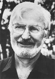
Heinrich Rohrer is a Swiss physicist who was one of three scientists to win the 1986 Nobel Prize in Physics. Rohrer shared one-half of the prize with physicist Gerd Binnig for their joint invention of the scanning tunneling microscope, which they developed while working as researchers at the IBM Research Laboratory in Zurich, Switzerland. Ernst Ruska was awarded the other half of the prize for his many contributions to electron microscopy.
Dr. Rohrer was born in Buchs, Switzerland, on 6 June 1933. He studied physics at the Swiss Federal Institute of Technology, receiving a bachelor’s degree in 1955 and a doctorate in 1960. He did post-doctoral work for two years at Rutgers University in New Brunswick, New Jersey, and in 1963 joined the IBM Research Laboratory in Zurich. In 1974-1975 he went to the University of California at Santa Barbara for a year-long sabbatical, and in 1986 he was appointed an IBM Fellow, the most prestigious technical position in the company. From 1986 to 1988 Dr. Rohrer served as the manager of the Zurich laboratory’s physical sciences department. He retired in July 1997.
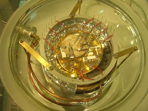
Rohrer and Binnig’s invention of the scanning tunneling microscope allowed scientists to image individual atoms for the first time. The microscope uses an extremely fine probe made out of tungsten to trace the surface of the material that is to be imaged. A quantum mechanical effect causes an electrical current to move between the tip of the probe and the surface, which can then be measured to determine the exact distance between the two. By recording the changes in the elevation of the tip as the probe is moved, a topographical map of the surface can be generated. The level of detail in the resulting map is fine enough that individual atoms may be clearly identified; later researchers have used variations on the device to physically move atoms from place to place.
Rohrer and Binnig have earned numerous awards for their invention, including the German Physics Prize, the Otto Klung Prize, and the Hewlett Packard Prize. The scanning tunneling microscope is now widely used in a wide variety of research applications in fields as diverse as semiconductor science, molecular biology, nanotechnology, and metallurgy.

