First-Hand:The AT&T BELLMAC-32 Microprocessor Development: Difference between revisions
(No difference)
| |
Revision as of 17:46, 13 May 2011
Contributed by Dr. Sung Mo (Steve) Kang, IEEE Fellow
For telecommunications services, AT&T Bell Laboratories first developed the 8-bit microprocessor chip BELLMAC-8 in the mid-1970s using 5 micron CMOS technology with its debut in 1977, followed by 4-bit microcomputer chip BELLMAC-4 using 3.5 micron CMOS technology in late 1970s. In 1974, however, the federal government started putting more pressure on AT&T to divide into two independent companies -- a long-distance telecommunications service company and another consisting of seven regional Bell operating companies (Baby Bells). Before agreeing to the divestiture, which happened on Jan. 1, 1984, AT&T asked to get into computer business and was allowed to do so. As a result of the request, the development of the next generation microprocessor chip, initially named BELLMAC-80, became critically important. A strategic decision was made for the architecture of BELLMAC-80 to be 32-bit instead of 16-bit chip, which would have been more gradual and prevented major surprises in development. Also, AT&T wanted the chip ready by 1980, another reason to call it BELLMAC-80. Thus, a serious project was initiated in late 1970s.
The development teams were located in three different locations: AT&T Bell Labs at Indian Hill, Naperville, Ill., which was known as the switching center of the world; AT&T Bell Labs at Holmdel, N.J., which had expertise in transmission aspects of telecommunications and architecture and logic design and circuit and AT&T Bell Labs at Murray Hill, N.J., known for expertise in circuit design, physical layout, CAD and fabrication technology.
My involvement in BELLMAC-80 started in 1978. After graduating from UC Berkeley in 1975, I taught at Rutgers University for two years before I joined AT&T Bell Labs at Holmdel in 1977. After spending a year in Holmdel to work on private network design, I asked to be relocated to AT&T Bell Labs at Murray Hill so that I could enter into the emerging field of MOS integrated circuits. Bernard Murphy, who was well known for his Murphy’s IC yield model,[1] was the department head in charge of microprocessor chip developments. He welcomed me into his department, specifically the high-end microprocessor design group that was to develop BELLMAC-80 using 3.5 micron twin-tub CMOS technology.[2] After careful analyses, the Integrated Circuits Laboratory of AT&T Bell Labs chose to use CMOS technology over NMOS technology based on power consumption as a key factor. This turned out to be the right decision. My initial project in Bernard Murphy’s department was to develop a library of CMOS standard cells for 3.5 micron twin-tub CMOS technology. There was a library of NMOS standard cells but nothing for CMOS.
I had to decide on a set of common parameters for standard cells, in particular, the uniform sizes of PMOS transistors (p-channel width) and NMOS transistors (n-channel width). For simple physical layout, uniform channel widths were preferred at that time, although this is not the case for modern standard cells. Based on noise margins, average speed of standard cells with typical fan out of three, and the silicon area occupied by standard cells, 35 micron was chosen for PMOSTs and 17 micron for NMOSTs. Many cells were designed for groups of NOR, NAND, inverter, D-latches and flip-flops with different fan-out capacities.[3] For accurate analysis of power consumption in CMOS integrated circuits that were better than C.Vdd.V.f, where V represents the voltage swing magnitude, I introduced a “power meter” for SPICE-type simulation.[4] The CAD environment assumed was for LTX for place-and-route, HCAP for parasitics and circuit extraction and MOTIS for timing simulation. At that time, the Computer Aides Laboratory under Herman Gummel’s directorship was at the leading edge of electronic CAD. A library was successfully developed for general use of LSI and MSI chip designs. For BELLMAC-32, these standard cells were planned for implementing “simple” control logic to interface with multiple programmable logic arrays (PLAs) and a 32-bit data path.
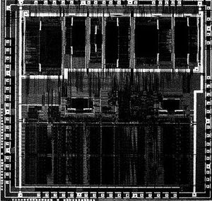
As was usually done for high-performance chips, the data path was tightly laid out using the gate-matrix layout format with metal wires run horizontally, whereas polysilicon wires run vertically bridged MOST gates with their interconnects contiguously. This concept was originally devised by Alex Lopez, a very knowledgeable layout expert, after many failed attempts to manually lay out a 32-bit data path in a given chip area. Without a sufficient automation tool, each chip designer had to use colored pencils to do the initial layout, which was then digitized by a program developed by Steve Law. Steve Law had talents in many areas including device physics, circuit design and software. Lopez and Law filed a patent application for the gate-matrix layout method.[5] Some novel circuit inventions were made, including “domino logic” and domino barrel shifter. At that time, Robert Krambeck supervised the high-end microprocessor design group and the initial concept for domino logic arose from his expertise in charge coupled device (CCD) principles. Domino circuit was co-invented by Robert Krambeck, Charles Lee and Steve Law.[6] A 32-bit barrel shifter was invented for fast shifting and rotation of 32 bits with masking in the data path using domino circuits.[7] Test chip fabrication of the data path was a huge success that yielded its speed far exceeding the target clocking frequency of 4MHz. Control logic implementation, however, turned out to be not as simple as originally hoped. Its complexity grew more and more and finally became tenfold more complex as the implementation neared its final stage. At that time, the world’s most advanced place-and-route tool, LTX, failed to handle 2,000 gates, which in today’s standard is laughably simple. Knowing no alternatives, Mean-Sea Tsay and I divided the control logic into two subgroups of 1,000 gates each and did manual placement using own graph-based heuristics and connected them with LTX, then patched two sub modules to PLAs and then to the data path. That was how the first BELLMAC-32 chip was developed. When the chip was fabricated and tested, the entire chip speed was hovering at 2MHz, the first lesson on speed bottleneck due to interconnects. This was a good achievement, but not a success according to AT&T’s computer business plan. The first project manager, Lee Thomas, was blamed for this failure. It was a very painful experience for team members at all three locations -- Naperville, Holmdel and Murray Hill.
The project, however, had to move on in order to meet performance goals. After numerous meetings and reviews, the development of BELLMAC-32A as a second-generation 32-bit microprocessor was put in motion. Developers chose a 2.5 micron twin-tub CMOS technology and the target clock frequency was set at 6.2MHz. Hing So of Holmdel was asked to oversee the project’s coordination. On the circuits and physical design side, I was put in charge of project coordination and scheduling. This time, the entire control layout was planned in gate-matrix layout format. Additionally, Masakazu Shoji was put in charge of designing clock trees and timing analysis. He completed numerous circuit-level ADVICE simulations to ensure the chip could run at the target clock frequency.[8] Thad Gabara did in-depth analysis of I/O circuits including transmission line effects at high operating frequencies.[9] Larry Nagel, who had developed the Berkeley SPICE program and worked in Herman Gummel’s laboratory, was in charge of ADVICE. Careful transistor size tuning and minimization of resistances in interconnects were critical in meeting numerous timing specifications.
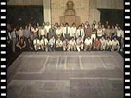
Chip layout verification was another huge challenge. At that time, no CAD tools were available for the entire chip layout verification. As a result, we had to generate many CALCOMP plots and Scotch-taped them together to form a 20-foot-by-20 foot plot that was placed on the floor in a huge room. To make sure interconnects were formed properly, all terminals were labeled and wires were traced by using color pencils to make sure the lines ran continually. Although primitive, this method uncovered many errors and, in the end, produced error-free layouts and fabricated chips.[10] We used a huge empty room in Building 3 of AT&T Bell Labs at Murray Hill or the main lobby area to complete the checking. After wafers were fabricated and tested, the fabrication yield was not as high as expected. To make a long story short, the then state-of-the-art tester Takeda Riken had serious transmission line problems that caused measurement errors. Mark Barber, the testing group supervisor, informed the manufacturer and summoned its engineering team to help correct the measurement errors.
Based on ADVICE simulation of the testing environment, we generated correction tables for timing test. When Mark Barber reported this problem in a test conference, his paper earned a best paper award that aroused the industry’s interest.[11] After correcting the test problems, many chips ran at frequencies higher than 6.2MHz -- many at 7, 8 and even 9MHz.
It took many man-months to develop BELLMAC-32 and its peripheral chips, but the technical accomplishments were historical and there was much to celebrate. Success in the laboratory, however, did not directly link to manufacturing success. After transferring all mask data to Western Electric Plant in Allentown, Pa., not much progress was made. Later, it was discovered that the chip was too complex to manufacture in Allentown, which was another big surprise. Glen Cheney, then director of Integrated Circuits Laboratory, ordered a task force to quench the fire. I formed a task force that consisted of a few key members of my high-end microprocessor design group, namely Wei-Tau Chiang, David Thompson and a few others. We commuted to Allentown daily over the next several months from Murray Hill. To build trust of the plant on our team, we started with “dirty” jobs such as sweeping the floor and calibrating test machines. The team building worked out well and after several months, Western Electric was able to produce more than the required number of good chips, thus completing the full development cycle. At that time, it was painfully obvious that in the factory environment with many Takeda Riken testers, machine-to-machine measurement variations were significant; another reality aspect that required design margins and that was very troublesome for reliability qualification. Also, there was no guarantee that the same machine would test chips after “baking” (thermal cycling). A technology update was done on BELLMAC-32A to produce WE32100, WE32200 and their peripheral chips. For each technology update project, the design team worked closely with the process development team, headed by Lou Parrillo who had invented the twin-tub CMOS process, as well as the process simulation team headed by Wolfgang Fichtner, who is now at ETH Zurich, in George Smith’s department. Incidentally, George Smith received the 2009 Nobel Prize in physics for his contribution to CCD devices. I remember hard negotiations with Lou Parrillo on design rules to achieve high packing density while Parrillo’s group tried hard to secure no shorts due to metal or contact features being too close to each other. For prediction of new technology influence on the next generation chips, Wolfgang Fichtner’s process simulation tools were useful to generate preliminary device models for ADVICE simulation.
The next step was linking manufacturing success to commercial computer business success. The gap was much wider and beyond what engineering teams could bridge. AT&T tried to work it out with Italian computer company Olivetti, then NCR, but was not able to compete in any major way. Engineering success was not a commercial success. After initial sales efforts by AT&T’s nascent computer systems organization, one of the suggested feedbacks was to change the byte ordering in the data path as an option, and we had to accommodate that request to honor the potential customer as king. But, it was not clear whether that particular request changed the potential customer’s decision. The power of marketing was painfully felt by the development team.
Following the task force’s enormous success, Western Electric demanded that Bernard Murphy’s department be moved to Allentown to be close to the manufacturing plant on Union Boulevard. As a result, Lou Parrillo and I planned to move with our families to Allentown. It was time of uncertainty at AT&T and Bell Labs with divestiture starting in January 1984. It was at this time that Professor Tim Trick, who was then department head of electrical and computer engineering at the University of Illinois at Urbana-Champaign, recruited me to Illinois where I restarted my academic career as a tenured professor in fall 1985.Other members such as Steve Law and Paul Schwarz in Bell Labs were recruited to help start Solomon Design Automation, the former body of today’s Cadence Design Systems. Wei-Tau Chiang went to Intel Corporation as a corporate CAD manager.
I learned a great deal from the BELLMAC-32 experience, which helped me in my subsequent academic career at the University of Illinois at Urbana-Champaign (UIUC). While at UIUC, nearly 100 graduate students under my advising completed their degrees in VLSI design and CAD areas. More than 50 Ph.D.s are working in the fields of VLSI design and CAD after learning from my AT&T experience in BELLMAC-32 development. The experience in the manufacturing environment taught me the importance of proper design margins to be secured in chip designs in order to ensure manufacturability and low cost through quality design and led me to write a textbook on CMOS IC design.[12]
For additional information on Dr. Kang, see his oral history.
References
- ↑ B. T. Murphy, “Cost-Size Optima of Monolithic Integrated Circuits,” Proc. Of the IEEE, vol. 52, pp. 1537-1545, 1964
- ↑ L. C. Parrillo, et al., US Patent 4,889,825, “Twin-Tub CMOS II-An Advanced VLSI Technology,” Dec. 26, 1989
- ↑ S. M. Kang, “A Design of CMOS Polycells for LSI Circuits,” IEEE Trans. On Circuits and Systems, vol. 28, no. 3, pp. 838-843, August 1981
- ↑ S. M. Kang, “Simulation of Power Dissipation in VLSI Circuits,” IEEE Journal of Solid-State Circuits, vol. 21, no. 5, pp. 889-891, Oct. 1986
- ↑ A. D. Lopez and H. F. Law, “A Dense Gate Matrix Layout Method for MOS VLSI,” IEEE Trans. On Electron Devices, vol. 27, no. 8, pp. 1971-1675, August 1980
- ↑ R. H. Krambeck, C. M. Lee and H. F. Law,” High-Speed Compact Circuits with CMOS,” IEEE J. of Solid-State Circuits, vol. 17, no. 3, pp. 614-619, June 1982
- ↑ S. M. Kang and R. H. Krambeck, US Patent 4,396,994,”Data Shifting and Rotating Apparatus,” August 2, 1983
- ↑ M. Shoji, “Elimination of Process-Dependent Clock Skew in CMOS VLSI,” IEEE J. of Solid-State Circuits, vol. 21, no. 5, pp. 875-880, October 1986
- ↑ T. Gabara and D. W. Thompson, “High Speed Low Power CMOS Transmitter-Receiver System,” Proc. Of the 1988 International Conf. on Computer Design, pp. 344-347, Oct. 1988"
- ↑ S. M. Kang, R. H. Krambeck, H. F. Law, and A. D. Lopez, ”Gate Matrix Layout of Random Control Logic in a 32-bit CMOS CPU Adaptable to Evolving Logic Design,” IEEE Trans. On Computer-Aided Design of Integrated Circuits and Systems, vol. 2, no. 1, pp. 18-29, January 1983
- ↑ Mark Barber, “Subnanosecond Timing Measurements on CMOS Devices Using Modern VLSI Test Systems,” International Test Conference, 1983
- ↑ S. M. Kang and Y. Leblebici, CMOS Integrated Circuits: Analysis and Design, 3rd edition, McGraw-Hill, 2003, 1999, 1996.
