First-Hand:Saving the Transistor Symbol
Saving the Transistor Symbol
Submitted by Sorab K. Ghandhi
The Transistor was invented by Bell Labs in late 1947, and announced to the public in 1948. This device had three semiconductor regions; an Emitter, a Base, and a Collector. In its original version, it comprised a slab of semiconductor material, germanium, mounted on a pedestal which served as the Base. Two tungsten wires pressed on its surface, and comprised the Emitter and Collector regions respectively.
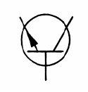
Its graphical symbol closely represented this device. The base was doped with impurities so that conduction through it was essentially by electrons, so it was referred to as n-type. The complete device was called a p-n-p transistor; its graphical symbol depicted an arrow on the emitter, pointed down into the base. See Fig. 1.
If the starting material for the base were p-type, the device would end up as an n-p-n transistor, and the emitter shown with the arrowhead pointed out away from the base. See Fig. 2
These were the symbols for a p-n-p and n-p-n transistor respectively. In either case, the symbol was depicted with a circle around it as an enclosure.
Over the years, Bell, and many other labs, proceeded to publish a number of papers on this device, including papers on transistor circuits. This symbol was universally accepted (after all, Bell Labs had invented the device) and was incorporated into thousands of documents (papers, specification sheets, instruction manuals, books, etc., etc.) all over the world. Our own books, Principles of Transistor Circuits and Transistor Circuit Engineering, edited by Dick Shea at General Electric (GE), made full use of this symbol. RCA and IBM chose initially a different depiction, but this was discontinued after a few years.
A major process improvement came when the Emitter and Collector were replaced by solid regions, thus avoiding the fragility of wires. This also allowed researchers to fabricate devices with extra regions to perform newer functions and we could now envision a day when this device could have multiple regions and/or terminals. This, in turn, led to the question: how can a graphical symbol be made to accommodate these new, yet-to-be-developed devices?
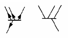
In 1957, the Symbols committee of the Institute of Radio Engineers (IRE) was asked to look into this problem, and brought in some transistor experts for this purpose, since their work primarily dealt with vacuum tubes, circuit breakers, capacitors, relays, transformers, etc. I was one of these transistor experts, and was appointed Chairman of this Task Group (28.4.8), since I had been working on these devices since 1953, when I joined GE, and knew more about these devices than any other transistor expert on our Group. We eventually developed an expandable scheme, which was tested for a couple of years by others in the technical community, to make sure it was fool proof. Some of the basic elements of this expandable scheme are shown in Figs. 3a-3c.
The primary advantage of this logical approach was that it degenerated to the classical Bell Labs symbol (Figs 1, 2) when only three regions that were involved, either p-n-p or n-p-n. The intention was to present this system to the International Standards Group and gain its world-wide acceptance. The next meeting of this committee was in the Summer of 1961, at Interlaken in Switzerland. We were pretty sure our system would be accepted, and took for granted that this would be the case.
But all was not well! In April 1961, three months before the meeting, Bob Pritchard (one of the leaders of the IRE Standards Committee), got wind of the fact that the French and Belgians had developed a system of their own, and planned to propose it as an alternative to ours. Bob sent me a copy, which I studied in detail. Their system depicted the transistor as a multi-grid vacuum tube, with solid and dashed grids for its many regions, and degenerated to that of a vacuum tube symbol in its three-region version. Moreover, it had a number of serious flaws, and I laid these out in the form of a rebuttal, which I sent to Bob. He, in turn, passed them on to Mr. Lange (a member of the GE turbine division, I believe), who was the USA representative at the 1961 meeting. Mr. Lange knew nothing about transistors, but we were confident we had a superior system which would speak for itself.
A month later, Bob came back with a horror story. He had picked up a rumor that all the other countries (13) had colluded to vote against the USA. Also, that Lange, in the spirit of brotherly openness, had passed my confidential rebuttal on to the Belgians and the French. At this point, Bob convinced the management of Philco, where I was working at that time, to send me to Switzerland to defend our system.
I arrived in Interlaken one day before the meeting, and went to Bern to visit my friend Andreas Bachmann, an ex-colleague from GE, who was a senior engineer with the PTT (Post and Telegraph) there. After a pleasant evening, he casually asked me for the purpose of my visit, and I told him. His reply: "Don’t be disappointed if you fail, Soli. Only yesterday, the other groups had a private meeting at PTT headquarters, and decided they would gang up against to the USA, 13:1, because they were upset by your arrogant attitude".
The Semiconductor Standards meeting was held in a kindergarten school which was commandeered for the purposes, and we sat on mini-desks during the next few days. I attended in the company of my senior representative, Lange, as his expert on semiconductors. The chairman opened the meeting in English, with the remark: "Since this is an International Conference, where French and English are the languages, I shall conduct the proceedings in French." Thunderstruck, I asked Lange (who knew French) for permission to address the chairman. Permission was granted, and I rose to say, in English, "Mr. Chairman, I am from India, and I know Hindustani, Hindi, Urdu, Gujerati, Latin and English, but I regret I do not know French". At which the chairman grandly said that he would conduct the Semiconductor part of the meeting in English out of respect for my situation. Whew! Throughout the entire meeting, I never even hinted that I was a US citizen.
I rose, and carefully outlined my system in detail, fending off occasional questions. It was clear to me that my main adversary was a German, a forceful individual by the name of Prof. Schönfeld. He seemed to know more about semiconductors than anyone else in the meeting.
During the coffee break, I had a chance to call aside the Belgian representative, and told him that I had prepared a rebuttal to his System. However, in the interest of fairness, I was going to give it to him to study so he would be prepared before our discussions. I knew that he already had seen my System, but he did not know that I knew, and was stunned by my generosity. "Dr. Ghandhi", he said, "you are indeed a gentleman". So, I had made one brownie point here, with a favorable impression on the Belgians.
Most of the meeting consisted of describing the US System, and trying to shoot it down, with no success. At one point, Prof. Schönfeld leaped up and said "Dr. Ghandhi, I have found a flaw in your system". I immediately saw that it was very minor, but before I could rebut him he added "But I also see a way around your problem", and proceeded to describe it. I decided to agree with him, saying, "Dr. Schönfeld, you have indeed found a flaw, and I am so glad you have come up with a solution. We shall now have to call this Schönfeld-US System". Dr. Schönfeld was delighted, and from here he became an ardent defender of our system. The next few days were spent attacking our system, which was so ably defended by Prof. Schönfeld, that I barely said another word.
We discussed the French-Belgian system over the next few days, but the tide had turned, and we came to the final vote. The Belgian said, "They will hang me in Brussels, but I shall vote for the US System." This started the bandwagon. All in favor, with only the French in opposition. The others pleaded with them to change their vote, in order to make it unanimous, with no luck. We had begun with a probable 1:13 and ended with a 13:1 in favor of the US system.
I left the meeting exhausted. My butt hurt from sitting on the small seats in the kindergarten where our session was held, and I barely got a glimpse of the Swiss Alps. Upon returning to the USA, I sent a detailed report to Bob Terhune, our committee chairman. His short, but sweet reply was, "C'est Magnifique".
Epilogue
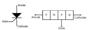
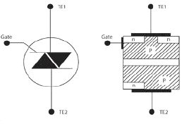
The Bell Labs version of the transistor symbol is now permanently established in the literature. Over the years, all the (very clever) multi-region variations of the transistor fell by the wayside, so that only a few of the innovative ideas in the "Schönfeld-US" system have been exploited. The only multi-region devices in use today are the four-region thyristor, and the five region bi-directional Triac.
I am still satisfied, however. You see, had the French system been accepted, we would be using a very different symbol for the commonly accepted one for the basic transistor, requiring many millions of documents to be altered in order to accommodate it.
About the Author
Sorab K. Ghandhi is an Emeritus Professor of Electrophysics, Rensselaer Polytechnic Institute, Troy NY, a Fellow of the IEEE, and the recipient of the 2010 IEEE EDS Education Award. He resides in Escondido, California USA and shares a love for Western classical music and for Mesoamerican archeology with his wife Cecille. He is indebted to Dr. Paul Agnello for providing supportive information for this manuscript and helping with the illustrations.


