Burn Jeng Lin: Difference between revisions
No edit summary |
No edit summary |
||
| (3 intermediate revisions by 2 users not shown) | |||
| Line 1: | Line 1: | ||
{{Biography | |||
|Image=Jeng Lin.jpg | |||
|Fields of study=Immersion lithography | |||
|Awards=[[IEEE Jun-ichi Nishizawa Medal]] | |||
}} | |||
Burn J. Lin is recognized as a technical leader in the [[Semiconductors|semiconductor]] manufacturing industry and most responsible for 193-nm immersion lithography. In 2002, Dr. Lin proposed immersion lithography, which is a resolution-enhancement process that replaces the air gap between the lens and the wafer surface with a liquid medium, such as purified water. Through Dr. Lin’s perseverance in convincing the industry that a change was needed, immersion lithography was adopted, and manufacturing of 45-nm feature sizes and smaller have become possible. | Burn J. Lin is recognized as a technical leader in the [[Semiconductors|semiconductor]] manufacturing industry and most responsible for 193-nm immersion lithography. In 2002, Dr. Lin proposed immersion lithography, which is a resolution-enhancement process that replaces the air gap between the lens and the wafer surface with a liquid medium, such as purified water. Through Dr. Lin’s perseverance in convincing the industry that a change was needed, immersion lithography was adopted, and manufacturing of 45-nm feature sizes and smaller have become possible. | ||
He has continued the cause for immersion lithography with groundbreaking papers that have mapped out scaling laws for super-high numerical aperture immersion optics, and he has led the development of defect-reduction methods to address concerns regarding the technology. As a result, immersion lithography has quickly become a manufacturing technology in just a few years. | He has continued the cause for immersion lithography with groundbreaking papers that have mapped out scaling laws for super-high numerical aperture immersion optics, and he has led the development of defect-reduction methods to address concerns regarding the technology. As a result, immersion lithography has quickly become a manufacturing technology in just a few years. | ||
Dr. Lin is an [[IEEE Fellow Grade History|IEEE Life Fellow]] and 2013 winner of the [[IEEE Jun-ichi Nishizawa Medal]] for "contributions to lithographic manufacturing, including immersion lithography." He is currently the senior director of the Nanopatterning Technology Division at TSMC, Ltd., the world’s largest silicon foundry. | |||
[[Category:Semiconductor device manufacture]] [[Category:Lasers, lighting & electrooptics]] [[Category:Optics]] | |||
{{DEFAULTSORT:Lin}} | |||
Latest revision as of 19:36, 19 January 2016
- Fields of study
- Immersion lithography
- Awards
- IEEE Jun-ichi Nishizawa Medal
Biography
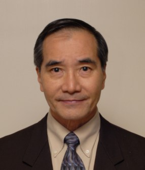
Burn J. Lin is recognized as a technical leader in the semiconductor manufacturing industry and most responsible for 193-nm immersion lithography. In 2002, Dr. Lin proposed immersion lithography, which is a resolution-enhancement process that replaces the air gap between the lens and the wafer surface with a liquid medium, such as purified water. Through Dr. Lin’s perseverance in convincing the industry that a change was needed, immersion lithography was adopted, and manufacturing of 45-nm feature sizes and smaller have become possible.
He has continued the cause for immersion lithography with groundbreaking papers that have mapped out scaling laws for super-high numerical aperture immersion optics, and he has led the development of defect-reduction methods to address concerns regarding the technology. As a result, immersion lithography has quickly become a manufacturing technology in just a few years.
Dr. Lin is an IEEE Life Fellow and 2013 winner of the IEEE Jun-ichi Nishizawa Medal for "contributions to lithographic manufacturing, including immersion lithography." He is currently the senior director of the Nanopatterning Technology Division at TSMC, Ltd., the world’s largest silicon foundry.
