Beam Lead Technology: Difference between revisions
No edit summary |
No edit summary |
||
| Line 11: | Line 11: | ||
<span></span><span>[BSTJ_Beam_Lead_Technology.pdf]</span>[[Image:BSTJ Beam Lead Technology.pdf|center|BSTJ article]][original IEEE paper.pdf][[Image:Original IEEE paper-1965.PDF|Image:Original_IEEE_paper-1965.PDF]]<br> | <span></span><span>[BSTJ_Beam_Lead_Technology.pdf]</span>[[Image:BSTJ Beam Lead Technology.pdf|center|BSTJ article]][original IEEE paper.pdf][[Image:Original IEEE paper-1965.PDF|Image:Original_IEEE_paper-1965.PDF]]<br> | ||
| [BSTJ air isolated crossovers.pdf] | ||
<u>Air-Isolated IC 1964 IEDM talk</u> | <u>Air-Isolated IC 1964 IEDM talk</u> | ||
Revision as of 14:39, 6 April 2009
Beam Lead Technology
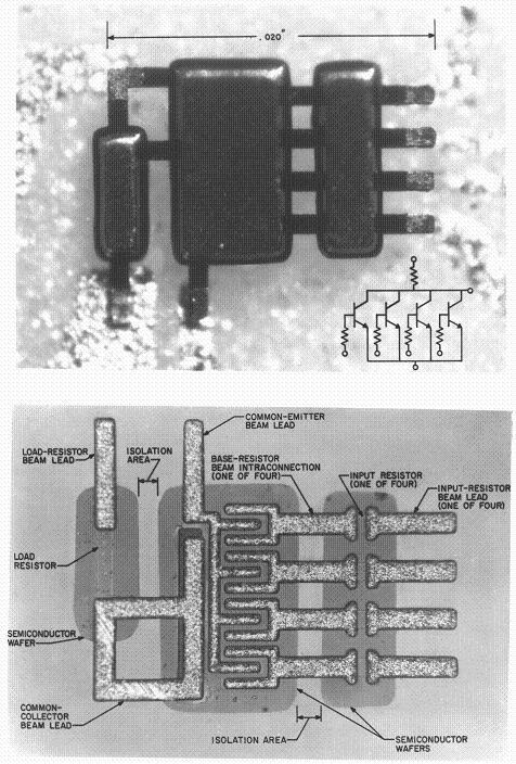
Beam Lead Technology is the name given to the structure and method of micro-fabricating a semiconductor device structure. Its original application was to high-frequency silicon switching transistors and ultra-high-speed integrated circuits. In the early 1960's M.P.Lepselter developed the techniques for fabricating a structure consisting of electroforming an array of thick, self-supporting gold patterns on a thin film Ti-Pt Au base, hence the name "beams", deposited on the surface of a silicon wafer . The excess semiconductor from under the beams was removed, thereby separating the individual devices and leaving them with self-supporting beam leads, or internal chiplets, cantilevered beyond the semiconductor. The contacts served as electrical leads in addition to serving the purpose of structural support for the devices.Today this micro-machining technology is also known as MEMS.
Legacy
This technology, also known as air-bridge technology, has established itself for its unsurpassed reliability in high-frequency silicon switching transistors and ultra-high-speed integrated circuits for telecommunications and missile systems. The Beam Lead devices, produced by the hundreds of millions, became the first example of a commercial microelectromechanical structure (MEMS).
Other omnipresent uses of Beam Lead Technology are the silicide process and structure (Schottky Diodes and contacts) used in every silicon integrated circuit today; plasma etching, and precision electro-forming, etc.
[BSTJ_Beam_Lead_Technology.pdf]File:BSTJ Beam Lead Technology.pdf[original IEEE paper.pdf]File:Original IEEE paper-1965.PDF
[BSTJ air isolated crossovers.pdf]
Air-Isolated IC 1964 IEDM talk
