Beam Lead Technology: Difference between revisions
(New page: == Beam Lead Technology == <br><meta content="text/html; charset=utf-8" http-equiv="Content-Type"></meta><meta content="Word.Document" name="ProgId"></meta><meta content="Microsoft Word ...) |
No edit summary |
||
| (38 intermediate revisions by 3 users not shown) | |||
| Line 1: | Line 1: | ||
== Beam Lead Technology == | == Beam Lead Technology == | ||
[[Image:Original IEEE Beam Lead Article-April 1965.jpg|thumb|right]] | |||
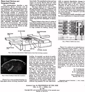
Beam Lead Technology is the name given to the structure and method of micro-fabricating a semiconductor device structure. Its original application was to high-frequency silicon switching transistors and ultra-high-speed integrated circuits. In the early 1960's [[Martin P. Lepselter|M.P. Lepselter]] developed the techniques for fabricating a structure consisting of electroforming an array of thick, self-supporting gold patterns on a thin film Ti-Pt Au base, hence the name "beams", deposited on the surface of a silicon wafer . The excess semiconductor from under the beams was removed, thereby separating the individual devices and leaving them with self-supporting beam leads, or internal chiplets, cantilevered beyond the semiconductor. The contacts served as electrical leads in addition to serving the purpose of structural support for the devices.Today this micro-machining technology is also known as [[MEMS |MEMS]]. | |||
== Legacy == | |||
[[Image:LOAD RESISTOR ISOLATION AIM Circuit.JPG|thumb|right]] | |||
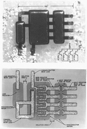
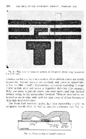
This technology, also known as air-bridge technology, has established itself for its unsurpassed reliability in high-frequency silicon switching transistors and ultra-high-speed integrated circuits for telecommunications and missile systems. The Beam Lead devices, produced by the hundreds of millions, became the first example of a commercial microelectromechanical structure (MEMS). A specific example of what is today called a MEMS device is the air isolated cross over, aka the "Lepselter Crossover",used in the ESS System. | |||
Other omnipresent uses of Beam Lead Technology are the silicide process and structure (Schottky Diodes and contacts) used in every silicon integrated circuit today; plasma etching, and precision electro-forming, etc. | |||
[[Image:BSTJ air isolated crossovers-deflection.jpg|thumb|right]] | |||
== References == | |||
1. "Beam-Lead Devices and Integrated Circuits", Electron Devices Meeting, October 29, 1964, Washington, D.C. | |||
2. M.P. Lepselter, et al,"[[Media:Original_IEEE_paper-1965.PDF|Beam-Lead Devices and Integrated Circuits]]," Proceedings of the IEEE, 53 (4) (1965), p.405. | |||
3. Lepselter, M. P., "Beam-lead Technology," Bell System Technical Journal Vol. 45, February 1966, pp: 233-253 | |||
4. Vibratory Reed Device, Boll & Lepselter, US Patent 3,609,593, filed May 25, 1966 | |||
5. Lepselter, M. P., "Beam Lead Sealed Junction Technology", Bell Laboratories. Record, Oct.-Nov. 1966, pp. 299-303. | |||
6. M. Lepselter et al., "Silicon Schottky Barrier Diode with Near-Ideal I-V Characteristics," B.S.T.J., Feb. 1968, pp.195-208 | |||
7. M.P. Lepselter, "Air-Insulated Beam-Lead Crossovers for Integrated Circuits", Bell System Technical Journal,<br>Vol. 47, Feb. 1968, p.269 <br> | |||
Beam Lead Technology is the name given to the structure and method of micro-fabricating a semiconductor device structure. Its original application was to high-frequency silicon switching transistors and ultra-high-speed integrated circuits. | |||
8. M.Lepselter, "Integrated circuits- the New Steel", International Electron Devices Meeting (IEDM)1974, IEDM Digest, Dec. 1974<br> | |||
---- | |||
[[Media:BSTJ_Beam_Lead_Technology.pdf|Original IEEE Beam Lead Article - April 1965]] | |||
[[Category:Integrated_circuits]] | |||
Revision as of 18:51, 14 March 2014
Beam Lead Technology
Beam Lead Technology is the name given to the structure and method of micro-fabricating a semiconductor device structure. Its original application was to high-frequency silicon switching transistors and ultra-high-speed integrated circuits. In the early 1960's M.P. Lepselter developed the techniques for fabricating a structure consisting of electroforming an array of thick, self-supporting gold patterns on a thin film Ti-Pt Au base, hence the name "beams", deposited on the surface of a silicon wafer . The excess semiconductor from under the beams was removed, thereby separating the individual devices and leaving them with self-supporting beam leads, or internal chiplets, cantilevered beyond the semiconductor. The contacts served as electrical leads in addition to serving the purpose of structural support for the devices.Today this micro-machining technology is also known as MEMS.
Legacy
This technology, also known as air-bridge technology, has established itself for its unsurpassed reliability in high-frequency silicon switching transistors and ultra-high-speed integrated circuits for telecommunications and missile systems. The Beam Lead devices, produced by the hundreds of millions, became the first example of a commercial microelectromechanical structure (MEMS). A specific example of what is today called a MEMS device is the air isolated cross over, aka the "Lepselter Crossover",used in the ESS System.
Other omnipresent uses of Beam Lead Technology are the silicide process and structure (Schottky Diodes and contacts) used in every silicon integrated circuit today; plasma etching, and precision electro-forming, etc.
References
1. "Beam-Lead Devices and Integrated Circuits", Electron Devices Meeting, October 29, 1964, Washington, D.C.
2. M.P. Lepselter, et al,"Beam-Lead Devices and Integrated Circuits," Proceedings of the IEEE, 53 (4) (1965), p.405.
3. Lepselter, M. P., "Beam-lead Technology," Bell System Technical Journal Vol. 45, February 1966, pp: 233-253
4. Vibratory Reed Device, Boll & Lepselter, US Patent 3,609,593, filed May 25, 1966
5. Lepselter, M. P., "Beam Lead Sealed Junction Technology", Bell Laboratories. Record, Oct.-Nov. 1966, pp. 299-303.
6. M. Lepselter et al., "Silicon Schottky Barrier Diode with Near-Ideal I-V Characteristics," B.S.T.J., Feb. 1968, pp.195-208
7. M.P. Lepselter, "Air-Insulated Beam-Lead Crossovers for Integrated Circuits", Bell System Technical Journal,
Vol. 47, Feb. 1968, p.269
8. M.Lepselter, "Integrated circuits- the New Steel", International Electron Devices Meeting (IEDM)1974, IEDM Digest, Dec. 1974


